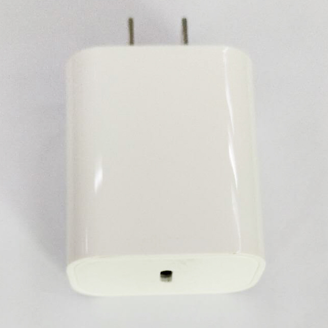
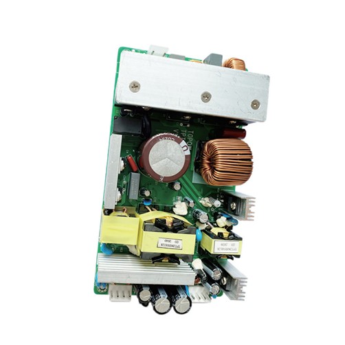
Model: TPT285D5412A
Input voltage range: 100~240Vac
Output voltage and current: Output 1: 54V/4.5A; Output 2: 12V/3A
Output Power: 285
Working temperature: -25℃~+50℃
Size: 170mm*95mm*32mm
Double output efficiency>91%
Output protection: OVP/OSP/OCP/OLP
RoHS compliant
IEC 60950/62368
EMI Class A
Leakage current is less than 3.5mA
Surge: common mode 6KV, differential mode 6KV
1. POWER SUPPLY OVERVIEW:
1.1 INPUT ELECTRICAL CHARACTERISTICS OVERVIEW
1.1.1 Input voltage range: 90Vac to 264Vac
1.1.2 Nominal input Normal voltage range: 100Vac to 240Vac
1.1.3 Standby power Loss: measured at 100Vac No load
1.1.4 Power Factor PF>0.95 (100-240Vac Input ,Full load)
1.1.5 Max input ac current: 4Amax at full load condition @90Vac~264Vac input
1.1.6 Inrush current: MAX80A (Cold start), 230Vac input
1.1.7 Input Power (W): 350W (max)@Full Load
1.1.8 Efficiency Efficiency: 91%(min) at 240VAC, full load condition;
1.1.9 Leakage Current: Less Than 3.5mA(max),230Vac input
1.1.10 Input Fuse: T15A/250Vac, T6.3A/250Vac
1.2 OUTPUT ELECTRICAL CHARACTERISTICS OVERVIEW
1.2.1 OUTPUT VOLTAGE RANGE
Output Voltage | Min value | Normal value | Max value | Requirements |
Vout1 | 53.4V | 54.5V | 55.6V | Vin=100Vac—240Vac Io=4.8A MaximumOutput Capacitance 470uF |
Vout2 | 11.4V | 12V | 12.6V | Vin=100Vac—240Vac Io=2A Maximum Output Capacitance 1000uF |
1.2.2 OUTPUT CURRENT RANGE
Output Current | Min value | Normal value | Max value | Requirements |
Iout1 | / | 4.8A | / | Vin=100Vac—240Vac |
Iout2 | / | 2A | / | Vin=100Vac—240Vac |
Note: Iout =0A, Criterion: No damage, hazardous, and resonance
1.2.3 LINE REGULATION
Line Regulation | Min value | Normal value | Max value | Requirements |
Vout1: 54.5V | / | ±1% | / | Vin=100Vac—240Vac Io=4.8A |
Vout2: 12V | / | ±1% | / | Vin=100Vac—240Vac Io=2A |
1.2.4 LOAD REGULATION
Load Regulation | Min value | Normal value | Max value | Requirements |
Vout1: 54.5V | / | ±2% | / | Vin=100Vac—240Vac Io=4.8A |
Vout2: 12V | / | ±2% | / | Vin=100Vac—240Vac Io=2A |
1.2.5 OUTPUT VOLTAGE TOLERANCE
Output voltage tolerance | Min value | Normal value | Max value | Requirements |
Vout1: 54.5V | / | / | ±2% | Vin=100Vac—240Vac Io=4.8A |
Vout2: 12V | / | / | ±5% | Vin=100Vac—240Vac Io=2A |
1.2.6 OUTPUT RIPPLE & NOISE
Output Voltage | Ripple & Noise (Max.) |
Vout1: 54.5V | 300mVp-p@0-50℃ |
Vout2: 12V | 120mVp-p@0-50℃ |
Note: 1) Measurements shall be made with an oscilloscope with 20MHz bandwidth.
2) Outputs shall be bypassed at the connector with a 0.1Uf ceramic capacitor and a 10Uf electrolytic capacitor to simulate system loading.
1.2.7 Output dynamic response
Voltage regulation | Slew Rate | Test Condition: Load Changing Scope |
54.5V ±5%; | 0.2A/us | 25% to 75% load and 75% to 25% load Frequence at 1KHz dwell time at 5ms |
12V ±5%; | 0.2A/us | 25% to 50% load and 50% to 75% load Frequence at 1KHz dwell time at 5ms |
1.2.8 OUTPUT OVERSHOOT / UNDERSHOOT
Output Overshoot / Undershoot | Min value | Normal value | Max value | Requirements |
Vout1: 54.5V | / | / | ±5% | Iout=0A-4.8A |
Vout2: 12V | / | / | ±5% | Iout=0A-2A |
1.2.9 TURN ON TIME
Turn on time | Min value | Normal value | Max value | Requirements |
Vout1: 54.5V | / | 2S | / | Vin=230Vac Io=4.8A |
Vout2: 12V | / | 2S | / | Vin=230Vac Io=2A |
1.2.10 OUTPUT HOLD TIME
Output Hold Time | Min value | Normal value | Max value | Requirements |
Vout1: 54.5V | / | 10mS | / | Vin=230Vac Io=4.8A |
Vout2: 12V | / | 10mS | / | Vin=230Vac Io=2A |
1.2.11 OUTPUT RISE TIME
output Rise time | Min value | Normal value | Max value | Requirements |
Vout1: 54.5V | / | 50ms | / | Vo=10%-90% Io=4.8A |
Vout2: 12V | / | 50ms | / | Vo=10%-90% Io=2A |
1.3 Protection function:
1.3.1 OUTPUT OVER CURRENT PROTECTION
Output over current Protection | Min value | Normal value | Max value | Requirements |
Vout1: 54.5V | 5.5A | / | 8A | Hiccup Auto-recovery mode |
Vout2: 12V | 2.5 A | / | 4A | Hiccup Auto-recovery mode |
1.3.2 OUTPUT SHORT CIRCUIT PROTECTION.
Output Short Circuit Protection | Comments |
Hiccup Auto-recovery mode |
1.3.3 OUTPUT OVER VOLTAGE PROTECTION
over voltage Protection | Min value | Normal value | Max value | Requirements |
Vout1: 54.5V |
56V |
/ |
61V
| Locked, can be restored after the fault is removed and restartedLatch |
Vout2: 12V |
13.5 |
/ |
15.6 |
Hiccup Auto-recovery mode |
2. Insulation performance ISOLATION
2.1 ISOLATION RESISTANCE
Requirements | Parameter value | Note |
500VDC/25℃/70%RH | ≥50MΩ | I/P-O/P,I/P-FG,O/P-FG |
2.2 ISOLATION WITHSTANDING VOLTAGE
Parameter name | Parameter value | Note |
Input To Output | 3000Vac/10mA/1min | No breakdown or flashover phenomenon |
Input To PG | 1500Vac/10mA/1min | No breakdown or flashover phenomenon |
Output To PG | 500Vac/10mA/1min | No breakdown or flashover phenomenon |
3. Safety requirements:
Design in accordance with UL60950 and EN60950 the requirements of the standard.
4. Electromagnetic compatibility EMC:
4.1 Electromagnetic Interference EMI
The power supply shall comply with the following Criterion:
1) Conduction Emission: EN55022, CLASS B
2) Radiated Emission: EN55022, CLASS B
3) Harmonics: *GB17625.1/ IEC/EN61000-3-2
4) Voltage flicker Flicker & Fluctuation: *GB17625.2/ IEC/EN 61000-3-3
4.2 Electromagnetic immunity EMS
The power supply shall comply with the following Criterion:
1) Electrostatic immunity ESD: *GB17626.2-1998/IEC61000-4-2/ EN 61000-4-2
2) Burst anti-interference EFT: *GB17626.4-1998/IEC61000-4-4 3KV /EN 61000-4-4,
3) Lightning surge Surge: *GB17626.5-1998/IEC61000-4-5 /EN 61000-4-5 Differential mode: 1KV Common mode: 2KV.
4) Voltage Dips: *EN 61000-4-11, IEC 1000-4-11:2001.
5) Radiation immunity RS: *GB17626.3-1998/IEC61000-4-3/ EN 61000-4-3
6) Conducted immunity CS: *GB17626.6-1998/IEC61000-4-6 /EN61000-4-6
7) Power frequency magnetic field immunity PMS: *GB17626.8-1998/IEC61000-4-8 /EN61000-4-8
5. Working environment ENVIRONMENTAL REQUIREMENT
5.1 Products life calculation MTBF
Over 300K hours at 25℃. And 100Vac under 100% Load (SR-332).7
Electrolytic capacitor life E-CAP life calculation MTBF
Lx=Lo*2^((To-Tx)/10) @ 50℃ (Over 50000 hours)
5.2 Ambient temperature
5.2.1 Operating temperature: -10℃ to +50℃.
5.2.2 Storage temperature: -20℃ to +70℃.
5.3 Ambient humidity
5.3.1 Operating: From 10%to90% relative humidity (non-condensing).
5.3.2 Store: From 5 to 95% relative humidity (non-condensing).
5.4 Altitude
5.4.1 Operating: to 5000m.
5.4.2 Store: to 5000m.
5.5 Cooling method: natural cooling.
5.6 Vibration test
10-55Hz, 49.0m/s²(5G), 3minutes period, 60minutes each along X, Y and Z axis.
5.7 Impact test
196.1m/s²(20G),11ms, once each X, Y and Z axis.
5.8 The derating curve is as follows:
")
6. Connector pin definition
7.1.Pin-CN1 DC Connection And Function TYPE: Vertical 3.96mm*3PIN
NO | Pin Connection | Function |
1 | L | L-INPUT |
2 | NG | NG |
3 | N | N-INPUT |
7.2. Vout1: Pin-CN5 DC Connection And Function TYPE: Vertical 3.96mm*4PIN
NO | Pin Connection | Function |
1 | 54.5V | RETURN |
2 | 54.5V | RETURN |
3 | GND | RETURN |
4 | GND | RETURN |
7.3.Vout2: Pin-CN4 DC Connection And Function TYPE: vertical 3.96mm*4PIN
NO | Pin Connection | Function |
1 | 12V | RETURN |
2 | 12V | RETURN |
3 | GND | RETURN |
4 | GND | RETURN |
8. Chart(Unit: mm)
9. Insulation sheet diagram
Remarks: 1. Two pieces of 20*20*5mm thermal pads should be added between the bottom of the power board and the switch case, with a thermal conductivity of ≥1.7W/m·K;
2. Steps to install the thermal pad: fix the insulating sheet on the four positioning posts of the case and close to the case, and cover the insulating sheet with the thermal pad
At the middle opening, finally put the power supply, and fix it on the four positioning posts of the case with screws.
10. Wire drawing
About

Product
Process
News
Recruitment

 中文
中文 Online consultation
 Online map
 中
中