Product

>
<

130W bare board power supply

TPT130D5412A


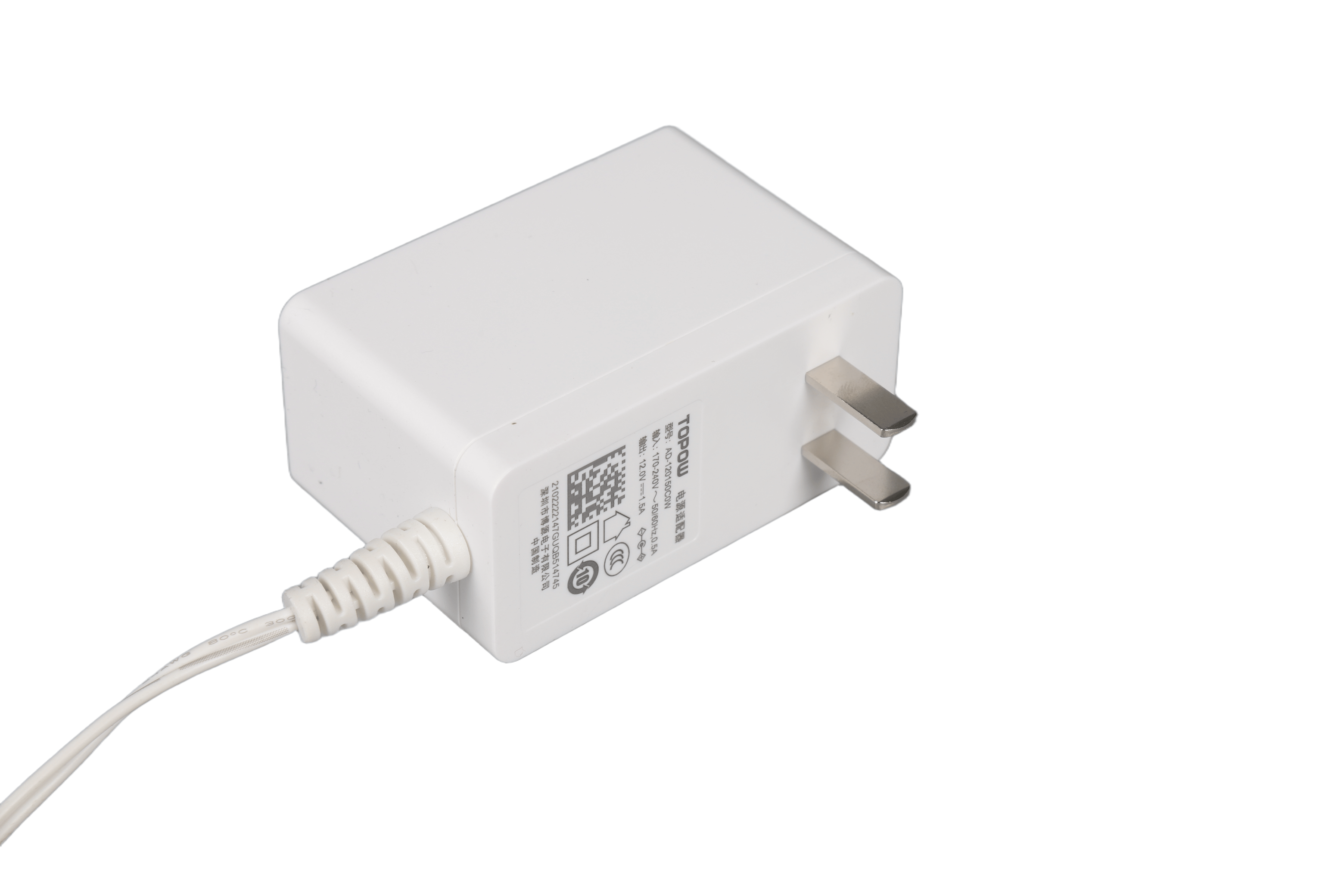
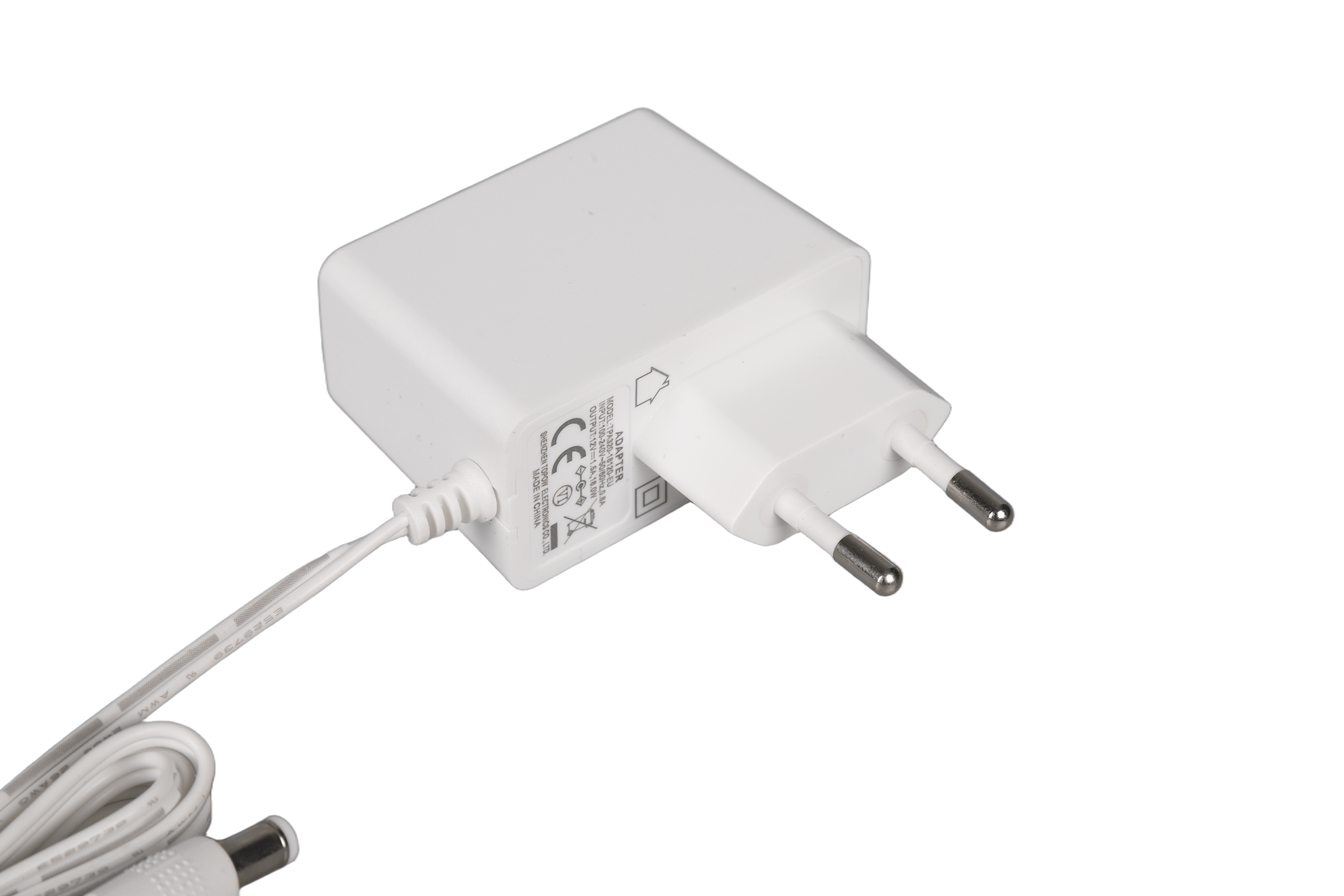
Product model: TPT130D5412A

Input voltage range: 100~240Vac

Output voltage and current: output 1: 54V/1.48A, output 2: 12V/1A

Working temperature: -10~+50℃

Size: 158mm*70mm*33mm

Double output efficiency> 85%

Output protection: OVP/OSP/OCP/OLP

RoHS compliant

IEC 60950/62368

EMI Class A

Leakage current is less than 3.5mA


Product Detail

1. POWER SUPPLY OVERVIEW:

1.1 INPUT ELECTRICAL CHARACTERISTICS OVERVIEW

1.1.1 Input voltage range: 90Vac to 264Vac

1.1.2 Nominal input Normal voltage range: 100Vac-240Vac

1.1.3 Standby power Loss: ≤2.0W at 100Vac No load

1.1.3 Full load input current Max input ac current: 2Amax at full load condition

1.1.4 Inrush current: MAX80A (Cold start), 230Vac input

1.1.5 Efficiency: 84% at 230Vac, full load condition;

1.1.6 Leakage Current: Less Than 3.5mA,230Vac input

1.1.7 Input Fuse: T5A/250Vac

1.2 OUTPUT ELECTRICAL CHARACTERISTICS OVERVIEW

1.2.1 OUTPUT VOLTAGE RANGE


Output Voltage


Min value


Normal value


Max value


Requirements

Vout1: 54V

53.4V

54V

54.6V

Vin=100Vac240Vac

Io=2.7A

Vout2: 12V

11.4V

12V

12.6V

Vin=100Vac240Vac

Io=1A

1.2.2 OUTPUT CURRENT RANGE


Output Current

Min value

Normal value

Max value

Requirements

Iout1

0A

/

2.7A

Vin=100Vac240Vac

Iout2

0A

/

1A

Vin=100Vac240Vac

1.2.3 LINE REGULATION

Line Regulation

Min value

Normal value

Max value

Requirements

Vout1: 54V

/

±1%

/

Vin=100Vac240Vac Io=2.7A

Vout2: 12V

/

±1%

/

Vin=100Vac~240Vac

Io=1A

1.2.4 LOAD REGULATION

Load Regulation

Min value

Normal value

Max value

Requirements

Vout1: 54V

/

±2%

/

Vin=100Vac~240Vac Io=2.7A

Vout2: 12V

/

±2%

/

Vin=100Vac~240Vac Io=1A

1.2.5 OUTPUT VOLTAGE TOLERANCE

Output voltage tolerance

Min value

Normal value

Max value

Requirements

Vout1: 54V

/

/

±5%

Vin=100Vac~240Vac Io=2.7A

Vout2: 12V

/

/

±5%

Vin=100Vac~240Vac Io=1A

1.2.6 OUTPUT RIPPLE & NOISE

Output Voltage

Ripple & Noise (Max.)

Vout1: 54V

500mVp-p@25

Vout2: 12V

120mVp-p@25

Note: 1) Measurements shall be made with an oscilloscope with 20MHz bandwidth.

2) Outputs shall be bypassed at the connector with a 0.1Uf ceramic capacitor and a 10Uf electrolytic capacitor to simulate system loading.

1.2.7 OUTPUT TRANSIENT RESPONSE

Voltage regulation

Slew Rate

Test Condition: Load Changing Scope

54V ±5%;

0.2A/us

25% to 50% load and 50% to 75% load

12V ±5%;

0.2A/us

25% to 50% load and 50% to 75% load

1.2.8 OUTPUT OVERSHOOT

Output Overshoot

Min value

Normal value

Max value

Requirements

Vout1:54V

/

/

±5%

Iout=0A-2.7A

Vout2:12V

/

/

±5%

Iout=0A-1A

1.2.9 TURN ON TIME

Turn on time

Min value

Normal value

Max value

Requirements

Vout1: 54V

/

3S

/

Vin=230Vac

Io=2.7A

Vout2: 12V

/

2S

/

Vin=230Vac

Io=1A

1.2.10 OUTPUT HOLD TIME

Output Hold Time

Min value

Normal value

Max value

Requirements

Vout1: 54V

/

10mS

/

Vin=100Vac  Io=2.7A

Vout2: 12V

/

10mS

/

Vin=100Vac  Io=1A

1.2.11 OUTPUT RISE TIME

Output Rise time

Min value

Normal value

Max value

Requirements

Vout1: 54V

/

20mS

/

Vo=10%-90% Io=2.7A

Vout2: 12V

/

20mS

/

Vo=10%-90% Io=1A

1.3 Protection function PROTECTION:

1.3.1 OUTPUT OVER CURRENT PROTECTION


Output over current Protection

Min value

Normal value

Max value

Requirements

Vout1: 54V

3.5A

/

5A

Hiccup  Auto-recovery mode

Vout2: 12V

1.2A

/

1.5A

Hiccup Auto-recovery mode

1.3.2 OUTPUT SHORT CIRCUIT PROTECTION.


Output Short Circuit Protection 

Comments


Hiccup  Auto-recovery mode

1.3.3 OUTPUT OVER VOLTAGE PROTECTION


Over voltage Protection

Min value

Normal value

Max value

Requirements

Vout1: 54V

58V

/

65V

Locked, can be restored after the fault is removed and restartedLatch

Vout2: 12V

/

/

/

Locked, can be restored after the fault is removed and restarted

Latch

1.3.4 OVER TEMPERATURE PROTECTION


Over temperature protection 

Temperature range

Comments


90℃±5

Since the recovery fault removing

2. Insulation performance ISOLATION

2.1 ISOLATION RESISTANCE

Requirements

Parameter value

Note

500VDC/25/70%RH

50MΩ

I/P-O/P,I/P-FG,O/P-FG

2.2 ISOLATION WITHSTANDING VOLTAGE

Parameter name

Parameter value

Note

Input To 54V

3000Vac/10mA/1min

No breakdown or flashover phenomenon

Input To 12V

3000Vac/10mA/1min

No breakdown or flashover phenomenon

Input To PG

1500Vac/10mA/1min

No breakdown or flashover phenomenon

54V To PG

500Vdc/10mA/1min

No breakdown or flashover phenomenon

12V To PG

500Vdc/10mA/1min

No breakdown or flashover phenomenon

54V To 12V

1500Vdc/10mA/1min

No breakdown or flashover phenomenon

3. Safety requirements:

The design meets the requirements of UL60950 and EN60950 standards.

 Design in accordance with UL60950 and EN60950 the requirements of the standard.

4. Electromagnetic compatibility EMC

4.1 Electromagnetic Interference EMI

The electromagnetic interference of the power supply meets the following rules:

The power supply shall comply with the following Criterion:

1) Conduction Emission: EN55022, CLASS B

2) Radiated Emission: EN55022, CLASS B

3) Harmonics: *GB17625.1/ IEC/EN61000-3-2

4) Voltage flicker Flicker & Fluctuation: *GB17625.2/ IEC/EN 61000-3-3


4.2 Electromagnetic immunity EMS

The electromagnetic immunity of the power supply meets the following rules:

The power supply shall comply with the following Criterion:

1) Electrostatic immunity ESD: *GB17626.2-1998/IEC61000-4-2/ EN 61000-4-2

2) Burst anti-interference EFT: *GB17626.4-1998/IEC61000-4-4 3KV /EN 61000-4-4,

3) Lightning surge Surge: *GB17626.5-1998/IEC61000-4-5 /EN 61000-4-5

   Differential mode: 6KV Common mode: 6KV.

 4) Voltage Dips: *EN 61000-4-11, IEC 1000-4-11:2001.

 5) Radiation immunity RS: *GB17626.3-1998/IEC61000-4-3/ EN 61000-4-3

 6) Conducted immunity CS: *GB17626.6-1998/IEC61000-4-6 /EN61000-4-6

 7) Power frequency magnetic field immunity PMS: *GB17626.8-1998/IEC61000-4-8 /EN61000-4-8

5. Working environment ENVIRONMENTAL REQUIREMENT

5.1 Products (E-CAP) life calculation MTBF

 Lx=Lo*2^((To-Tx)/10) @ 25℃ 5 Year (Over 44000 hours)

5.2 Ambient temperature

5.2.1 Operating temperature Operating: -10℃ to +40℃.

5.2.2 Storage temperature Store: -20℃ to +70℃.

5.3 Humidity

5.3.1 Operating: From 10%to90% relative humidity (non-condensing).

5.3.2 Store: From 5 to 95% relative humidity (non-condensing).

5.4 Altitude

5.4.1 Operating: to10,000 ft.

5.4.2 Store: to 20,000ft.

5.5 Cooling Method:

      Natural cooling Ventilation cooling.

5.6 Vibration Testing

10-55Hz, 49.0m/s²(5G), 3minutes period, 60minutes each along X, Y and Z axis.

5.7 Impact Testing

196.1m/s²(20G),11ms, once each X, Y and Z axis.


6. Connector pin definition

7.1.Pin-CON1 AC Connection And Function TYPE: vertical 3.96.0MM*3PIN hollow

NO

Pin Connection

Function

1

L

L-INPUT

2

/

/

3

N

N-INPUT

7.2.Pin-CON2 Connection And Function TYPE: 3.96MM*4PIN

NO

Pin Connection

Function

1

GND

54V RETURN

2

GND

54V RETURN

3

+54V

54V OUTPUT

4

+54V

54V OUTPUT

7.3. Pin-CON3 Connection And Function TYPE: 3.96MM*2PIN

NO

Pin Connection

Function

1

GND

12V RETURN

2

+12V

12V OUTPUT

7. Block schematic diagram

8. Curve

8.1 Temperature graph

130W bare board power supply(图1)
8.2 Derating curve
130W bare board power supply(图2)

9. Weight:

10. Chart(Unit: mm)

10.1 Wire dtawing

   10.1.1 AC Input figure: see Annex 1

10.1.2 DC Output figure: see Annex 2

    1) 54V Output figure: see Annex 3

    2) 12V Output figure: see Annex 4

10.2 Terminal figure

   10.2.1 AC Input Terminal figure: see Annex 5

10.2.2 DC Output Terminal figure: see Annex 6

    1) 54V Output Terminal figure: see Annex 7

    2) 12V Output Terminal figure: see attachment 8

10.3 The radiator dtawing: see Annex 9

10.4 Dimension: 127mm X 76.2mm X 33mm

10.5 Outline dimensions (Tolerance: ±0.5mm)

130W bare board power supply(图3)

11.Laout diagram

11.1 Bottomlayer: see appendix 10

11.2 Top silk screen Toplayer: see attachment 11

12. Label Label: see attachment 12

13. List of key components: see appendix 13