Product

>
<

Switching power supply pcb design output 164W power 90 - 264v ac adapter 54v 12v dc power supply

TPT164D5412A


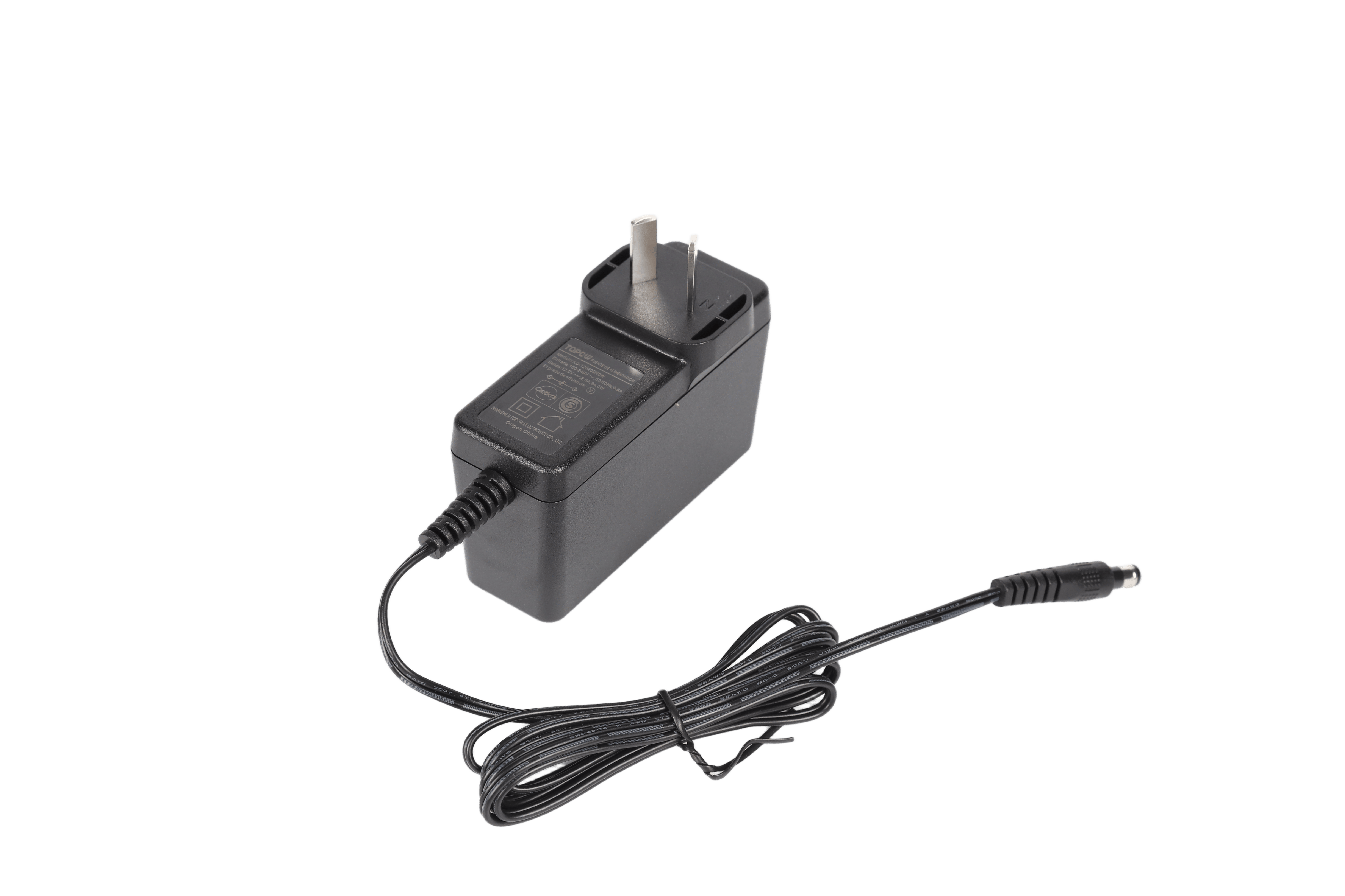
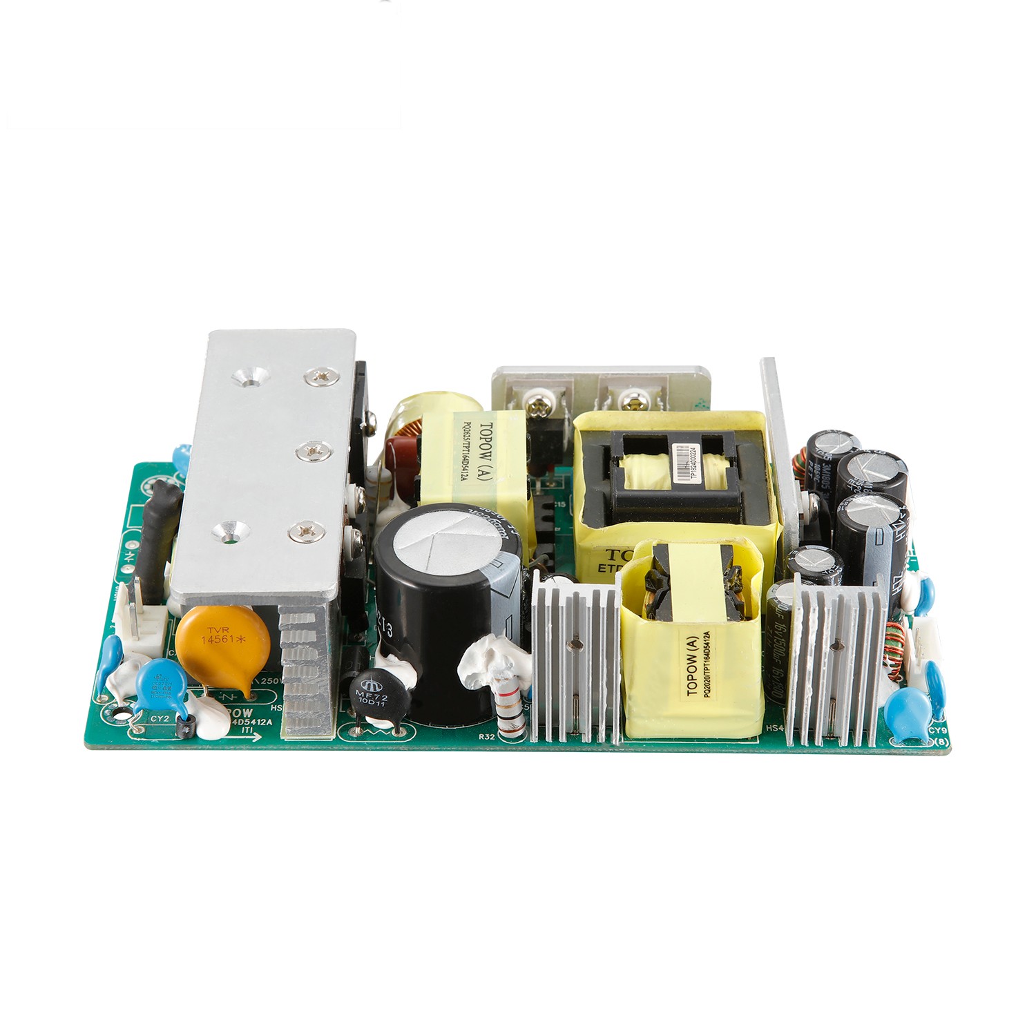
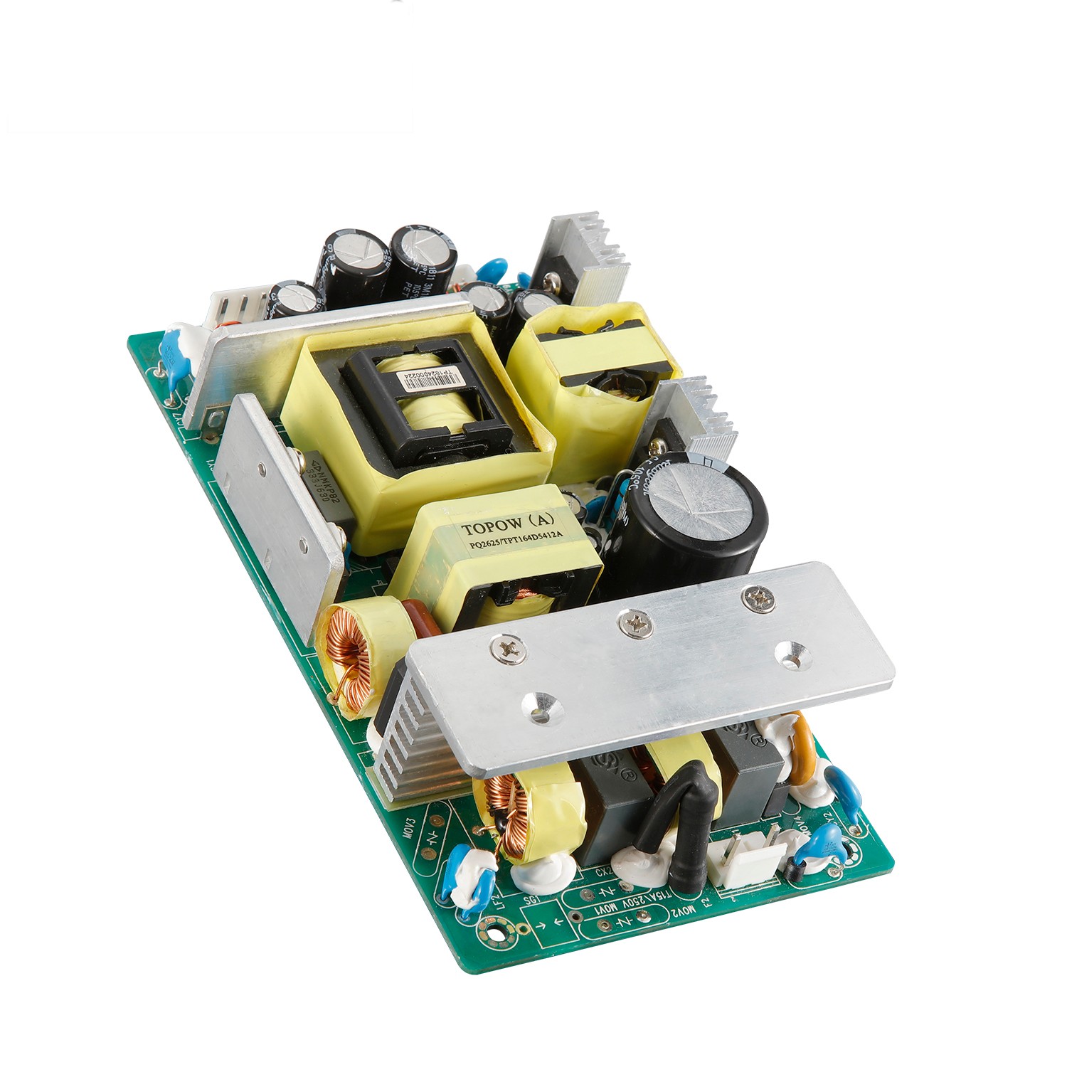
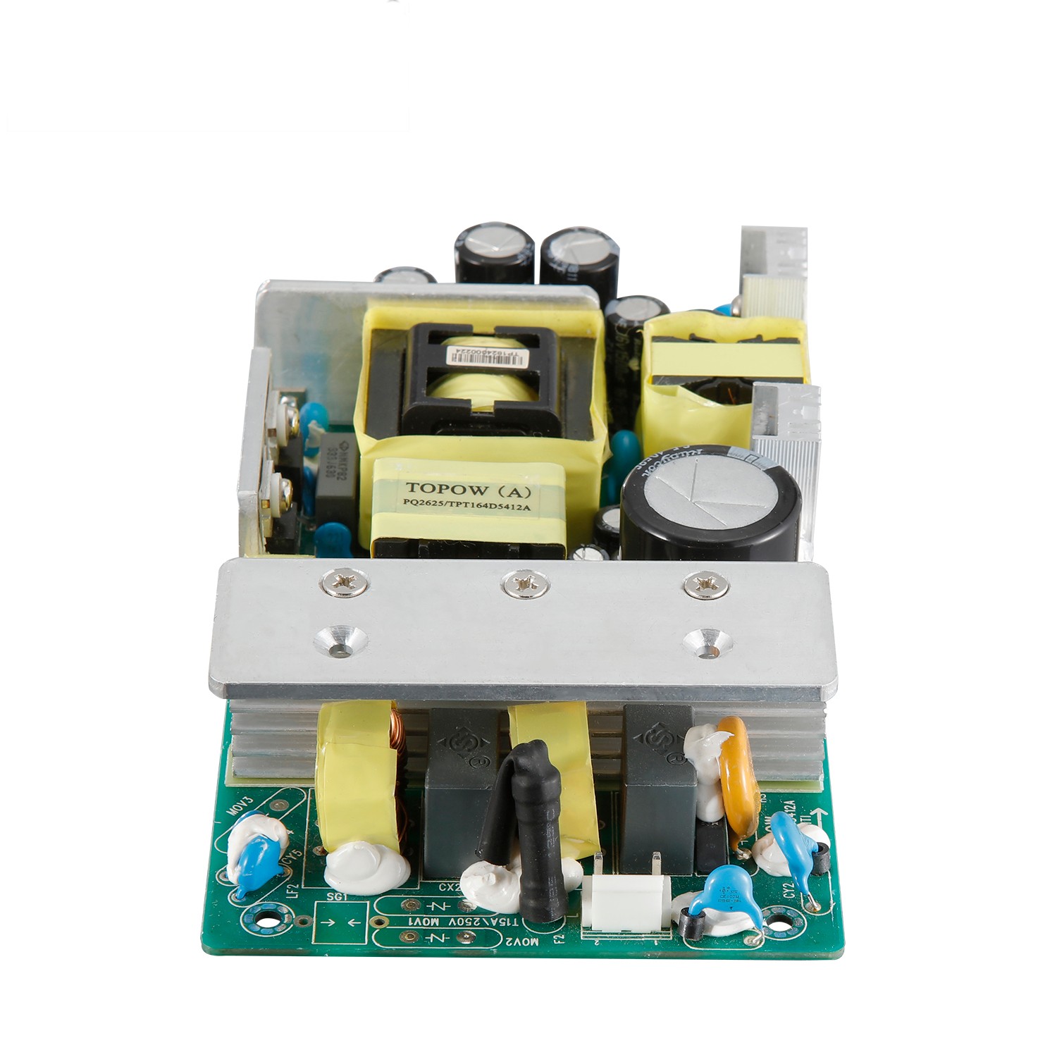
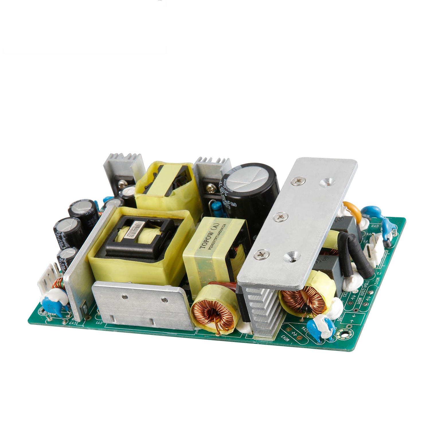
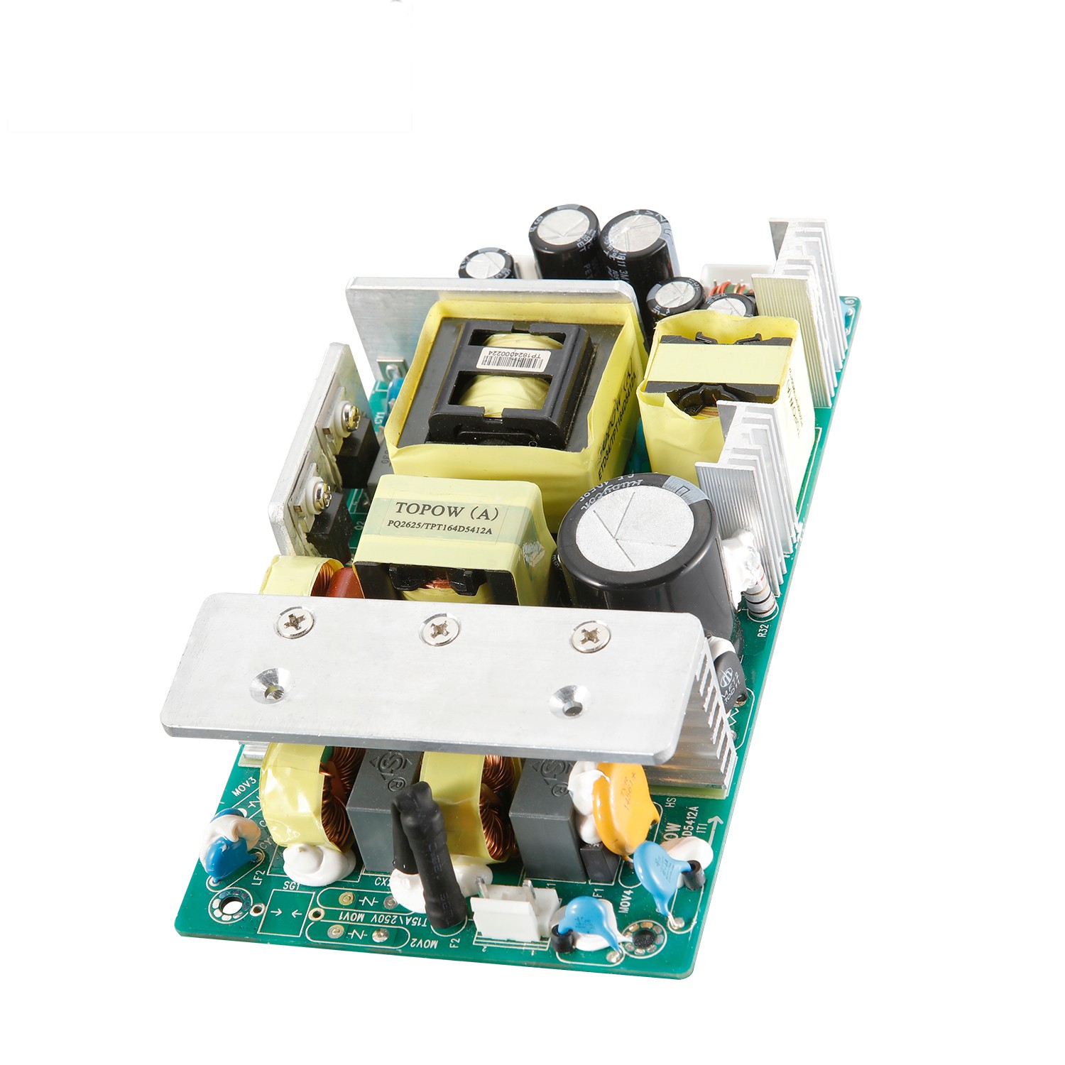
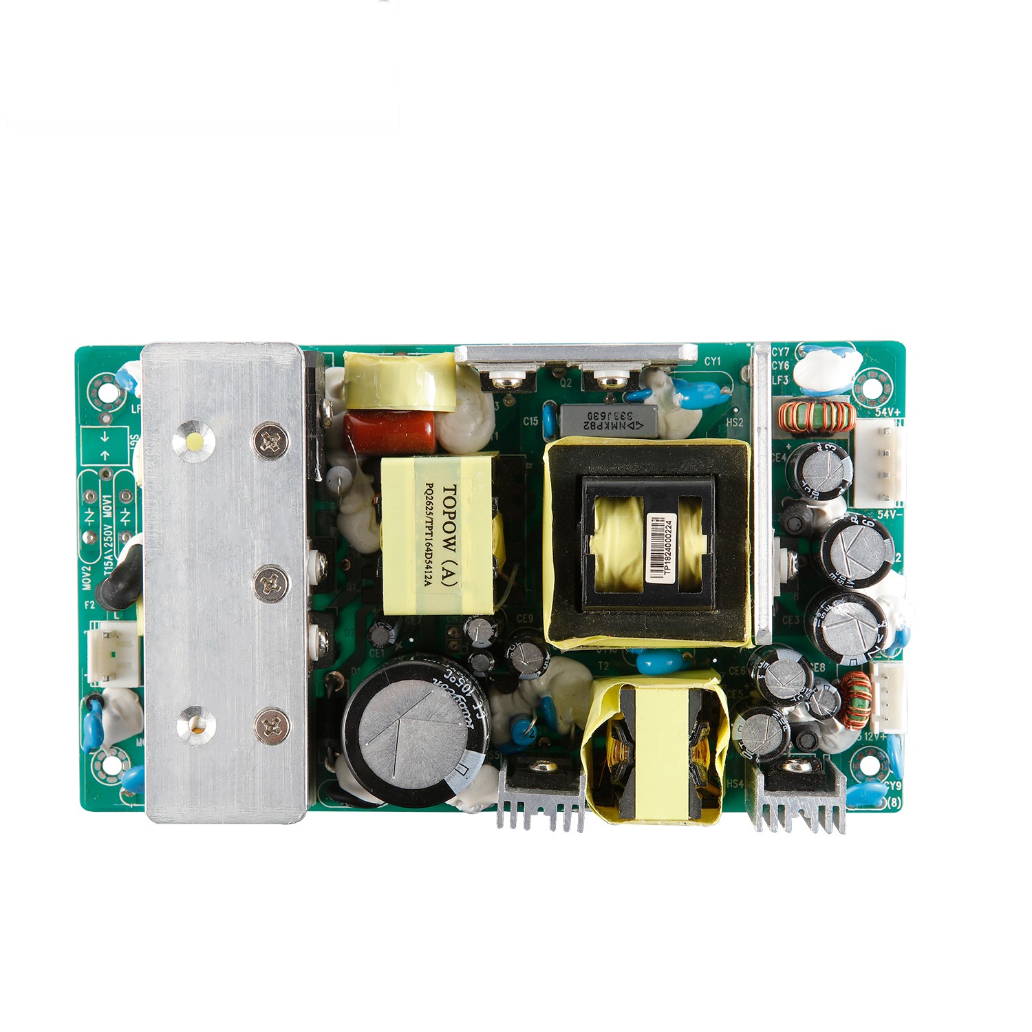
Power supply type: bare board

Output power: 164W

Output type (single or multiple groups?): Double groups

Input voltage: 90~264VAC

Input frequency: 47~63Hz

Output voltage/current: 54V/2.6A 12V/2

Mean time between failures: at least 200,000 hours

Protection: overcurrent and overvoltage

Efficiency: more than 88%

Inrush current: 80A/220VAC

Working temperature: -10~+50°C

Warranty period: 2 years


Product Detail

1. Electrical performance indicators:

1.1 INPUT ELECTRICAL CHARACTERISTICS OVERVIEW

1.1.1 Input voltage: 90Vac to 264Vac

1.1.2 Nominal input: 100Vac to 240Vac

1.1.3 Standby power consumption: measured at 100Vac No load

1.1.4 Power factor PF>0.95 (100-240Vac Input ,Full load)

1.1.5 Full load input current: 2.6Amax at full load condition @90Vac~264Vac input

1.1.6 Inrush current: MAX80A (Cold start), 230Vac input

1.1.7 Input power (W): 200W (max)@Full Load

1.1.8 Efficiency: 88%(min) at 240VAC, full load condition;

1.1.9 Leakage current: Less Than 3.5mA(max), 230Vac input

1.1.10 Input insurance: T15A/250Vac, T5A/250Vac

1.2 OUTPUT ELECTRICAL CHARACTERISTICS OVERVIEW

1.2.1 OUTPUT VOLTAGE RANGE

Output Voltage

Min value

Normal value

Max value

Requirements

Vout1

52.92V

54V

55.08V

Vin=100Vac240Vac

      Io=2.6A MaximumOutput Capacitance 470uF

Vout2

11.4V

12V

12.6V

Vin=100Vac240Vac

Io=2A

Maximum Output Capacitance 1000uF

1.2.2 OUTPUT CURRENT RANGE

Output Current

Min value

Normal value

Max value

Requirements

Iout1

/

2.6A

/

Vin=100Vac240Vac

Iout2

/

2A

/

Vin=100Vac240Vac

Note: Iout =0A, Criterion: No damage, hazardous, and resonance

1.2.3 LINE REGULATION


Line Regulation

Min value

Normal value

Max value

Requirements

Vout1: 54V

/

±1%

/

Vin=100Vac240Vac

Io=2.6A

Vout2: 12V

/

±1%

/

Vin=100Vac240Vac

Io=2A

1.2.4 LOAD REGULATION


Load Regulation

Min value

Normal value

Max value

Requirements

Vout1: 54V

/

±2%

/

Vin=100Vac240Vac

 Io=2.6A

Vout2: 12V

/

±2%

/

Vin=100Vac240Vac

 Io=2A

1.2.5 OUTPUT VOLTAGE TOLERANCE

Output voltage tolerance

Min value

Normal value

Max value

Requirements

Vout1: 54V

/

/

   ±2%

Vin=100Vac240Vac Io=2.6A

Vout2: 12V

/

/

   ±5%

Vin=100Vac240Vac Io=2A

1.2.6 OUTPUT RIPPLE & NOISE

Output Voltage

Ripple & Noise (Max.)

Vout1: 54V

300mVp-p@0-50

Vout2: 12V

120mVp-p@0-50

Note: 1) Measurements shall be made with an oscilloscope with 20MHz bandwidth.

2) Outputs shall be bypassed at the connector with a 0.1Uf ceramic capacitor and a 10Uf electrolytic capacitor to simulate system loading.

1.2.7 OUTPUT TRANSIENT RESPONSE

Voltage regulation

Slew Rate

Test Condition: Load Changing Scope

54V ±5%;

0.2A/us

20% to 80% load and 80% to 20% load

  Frequence at 1KHz dwell time at 5ms

12V ±5%;

0.2A/us

25% to 50% load and 50% to 75% load

Frequence at 1KHz dwell time at 5ms

1.2.8 OUTPUT OVERSHOOT / UNDERSHOOT

Output

Overshoot / Undershoot

Min value

Normal value

Max value

Requirements

Vout1: 12V

/

/

±5%

Iout=0A-2.A

Vout2: 54V

/

/

±5%

Iout=0A-2.6A

1.2.9 TURN ON TIME

Turn on time

Min value

Normal value

Max value

Requirements

Vout1: 54V

/

2S

/

Vin=230Vac

Io=2.6A

Vout2: 12V

/

2S

/

Vin=230Vac

Io=2A

1.2.10 OUTPUT HOLD TIME

Output Hold Time

Min value

Normal value

Max value

Requirements

Vout1: 54V

/

10mS

/

Vin=230Vac

Io=2.6A

Vout2: 12V

/

10mS

/

Vin=230Vac

Io=2A

1.2.11 OUTPUT RISE TIME

output Rise time

Min value

Normal value

Max value

Requirements

Vout1: 54V

/

50ms

/

Vo=10%-90% Io=2.6A

Vout2: 12V

/

50ms

/

Vo=10%-90% Io=2A

1.3 Protection function:

1.3.1 OUTPUT OVER CURRENT PROTECTION

Output over current Protection

Min value

Normal value

Max value

Requirements

Vout1: 54V

3.6A

/

5.2A

Hiccup  Auto-recovery mode

Vout2: 12V

2.5 A

/

4A

Hiccup  Auto-recovery mode

1.3.2 OUTPUT SHORT CIRCUIT PROTECTION.

Output Short Circuit Protection 

Comments


Hiccup  Auto-recovery mode

1.3.3 OUTPUT OVER VOLTAGE PROTECTION

over voltage Protection

Min value

Normal value

Max value

Requirements


Vout1: 54V


58.3V


/


62V


Hiccup  Auto-recovery mode


Vout2: 12V


13.5


/


15.6

Hiccup  Auto-recovery mode 

2. Insulation performance ISOLATION

2.1 ISOLATION RESISTANCE

Requirements

Parameter value

Note

500VDC/25/70%RH

50MΩ

I/P-O/P,I/P-FG,O/P-FG

2.2 ISOLATION WITHSTANDING VOLTAGE


Parameter name

Parameter value

Note

Input To Output

3000Vac/10mA/1min 

No breakdown or flashover phenomenon

Input To PG

1500Vac/10mA/1min

No breakdown or flashover phenomenon

Output To PG

500Vac/10mA/1min

No breakdown or flashover phenomenon


3. Safety requirements:

The design meets the requirements of UL60950 and EN60950 standards.

Design in accordance with UL60950 and EN60950 the requirements of the standard.

4. Electromagnetic compatibility EMC:

4.1 Electromagnetic Interference EMI

The power supply shall comply with the following Criterion:

1) Conduction Emission: EN55022, CLASS B

2) Radiated Emission: EN55022, CLASS B

3) Harmonics: *GB17625.1/ IEC/EN61000-3-2

4) Voltage flicker Flicker & Fluctuation: *GB17625.2/ IEC/EN 61000-3-3

4.2 Electromagnetic immunity EMS

The electromagnetic immunity of the power supply meets the following rules:

1) Electrostatic immunity ESD: *GB17626.2-1998/IEC61000-4-2/ EN 61000-4-2

2) Burst anti-interference EFT: *GB17626.4-1998/IEC61000-4-4 3KV /EN 61000-4-4,

3) Lightning surge: *GB17626.5-1998/IEC61000-4-5 /EN 61000-4-5 differential mode: 1KV common mode: 2KV.

4) Voltage drop: *EN 61000-4-11, IEC 1000-4-11:2001.

5) Radiation immunity RS: *GB17626.3-1998/IEC61000-4-3/ EN 61000-4-3

6) Conducted immunity CS: *GB17626.6-1998/IEC61000-4-6 /EN61000-4-6

7) Power frequency magnetic field immunity PMS: *GB17626.8-1998/IEC61000-4-8 /EN61000-4-8

5. Working environment

5.1 Products life calculation MTBF

Over 900K hours at 25℃. And 100Vac under 100% Load (SR-332).7

Electrolytic capacitor life E-CAP life calculation MTBF

Lx=Lo*2^((To-Tx)/10) @ 50℃ (Over 50000 hours)

5.2 Ambient temperature

5.2.1 Operating temperature: -10℃ to +50℃.

5.2.2 Storage temperature: -20℃ to +70℃.

5.3 Ambient humidity

5.3.1 Operating: From 10%to90% relative humidity (non-condensing).

5.3.2 Store: From 5 to 95% relative humidity (non-condensing).

5.4 Altitude

5.4.1 Operating: to 5000m.

5.4.2 Store: to 5000m.

5.5 Cooling method: natural cooling.

5.6 Vibration test

10-55Hz, 49.0m/s²(5G), 3minutes period, 60minutes each along X, Y and Z axis.

5.7 Impact test

196.1m/s²(20G),11ms, once each X, Y and Z axis.

 5.8 The derating curve is as follows:

Switching power supply pcb design output 164W power 90 - 264v ac adapter 54v 12v dc power supply(图1)

6. Connector pin definition

7.1.Pin-CN1 DC Connection And Function TYPE: Vertical 3.96mm*3PIN

NO

Pin Connection

Function

1

L

L-INPUT

2

NG

NG

3

N

N-INPUT

7.2. Vout1: Pin-CN2 DC Connection And Function TYPE: Vertical 3.96mm*4PIN

NO

Pin Connection

Function

1

GND

RETURN

2

GND

RETURN

3

54V

RETURN

4

54V

RETURN

7.3.Vout2: Connection And Function TYPE: Vertical 2.54mm*4PIN

NO

Pin Connection

Function

1

12V

RETURN

2

12V

RETURN

3

GND

RETURN

4

GND

RETURN

8. Chart(Unit: mm)
Switching power supply pcb design output 164W power 90 - 264v ac adapter 54v 12v dc power supply(图2)

Remarks: 1. A 52*62*6mm thermal pad should be added between the bottom of the power board and the switch case, with a thermal conductivity ≥1.7W/m·K;

2. Steps to install the thermal pad: fix the insulating sheet on the four positioning posts of the case and close to the case, and cover the insulating sheet with the thermal pad

At the middle opening, finally put the power supply, and fix it on the four positioning posts of the case with screws.

9. Wire drawing

9.1 Vout1:

Switching power supply pcb design output 164W power 90 - 264v ac adapter 54v 12v dc power supply(图3)
9.2 Vout2:
Switching power supply pcb design output 164W power 90 - 264v ac adapter 54v 12v dc power supply(图4)